

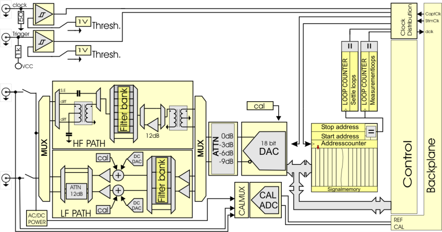
The AWG18 is an 18 bit Arbitrary Waveform Generator for high-speed / high resolution waveform generation. This module features two dedicated signal paths. A DC to 100 MHz path which is optimized for accurate time domain and frequency domain measurements up to 30 MHz. And a dedicated AC path optimized for signals between 10 MHz to 100 MHz. In combination with the built-in filters it features a typical harmonics level of better than -80 dBc for the whole range.
The module features differential outputs with a programmable common-mode voltage. For single ended applications the positive output as well as the negative output can be used. The clock can come from the backplane or from the front panel.
The module has 8 output ranges in steps of -3 dB, which covers a wide range of Unit Under Test input voltages.
The unit is an excellent choice when exceptional signal integrity in combination with a high level accuracy is required. The 8M-word (16M-byte) waveform memory allows very complex signal shapes to be generated. For higher output frequencies the waveform can be improved by using the x2 or x4 interpolation modes, resulting in maximum sample frequencies of 600 MS/s or 1.2 GS/s respectively.
The LF path combines high DC accuracy and fast level settling with an excellent dynamic signal performance up to 30 MHz. This allows precision time domain measurements as well as high quality dynamic measurements. The 10 MHz to 100 MHz signal path excels in dynamic signal generation. It features a filter-bank with 7 Low Pass filters, if desired the user can change any filter module with a custom version allowing an even better dynamic performance at user specific frequencies.
The jitter added to the applied front- or backplane clock is typically less than 0.2 ps.
Block Diagram
Key Features
- 300 MHz max. sample speed
- 600 MS/s and 1.2 GS/s interpolation modes
- 18 bit resolution
- Differential or Single Ended outputs
- 8 output ranges / 7 output filters
- Selectable filters to improve signal quality
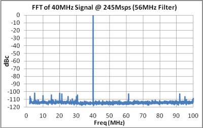
- -105 dBc THD typical at 10 MHz
- -78 dBc THD typical at 100 MHz
- 73 dBc SNR typical
- Programmable common mode voltage
- For ATX series hardware platform
Downloads
Technical Specifications
General
| Resolution | 18 bit |
| Update rate | 1 MHz - 300 MHz |
| Pattern memory depth | 8M words |
Output characteristics LF Path
| Output impedance | 50 Ohm |
| Ranges Single Ended (Vpp into open circuit) | 0.58 V, 0.82 V, 1.16 V, 1.64 V, 2.32 V, 3.28 V, 4.64 V, 6.56 V |
| Output filters (3 pole Butterw.) | Bypass, 15 MHz, 30 MHz |
| Bandwidth, -3 dB (typical) | 100 MHz (excl. sinx/x effect) |
| 0.1 dB flatness (typical) | 30 MHz (excl. sinX/X effect) |
| Output configuration | Differential, Single Ended |
| Output operating range | +/- 5.84 V |
Dynamic characteristics LF Path
(2 Vpp @ 50 Ohm single output, 250 MS/s, BW DC-100 MHz)| SNR (fout = 1 MHz) | 73 dBc |
| SNR (fout = 10 MHz) | 70 dBc |
| THD (fout = 1 MHz) | -90 dBc |
| THD (fout = 10 MHz) | -75 dBc |
| SFDR (fout = 1 MHz) | 92 dBc |
Accuracy (filter bypass)
| Absolute accuracy | ±(300 μV + 0.02 % of range) |
| Non Linearity | ±0.004 % of range |
Common mode voltage source
| Resolution | 16 Bit |
| Voltage range | -2.56 V to +2.56 V |
| DC-offset accuracy | ±(100 μV + 0.005 % of value) |
| Non Linearity | ±0.004 % of range |
| Non Linearity | ±100 ppm of range |
| Temperature drift (typical) | ±(10 ppm of range + 20 ppm of value)/ºC |
Output characteristics HF Path
| Output impedance | 50 Ω/ 100 Ω |
| Ranges Single Ended (Vpp into 50 Ohm) | 0.41 V, 0.58 V, 0.82 V, 1.16 V, 1.64 V, 2.32 V, 3.28 V, 4.63 V |
| Ranges differential (Vppdiff into 100 Ohm) | 0.58 V, 0.82 V, 1.16 V, 1.64 V, 2.32 V, 3.28 V, 4.64 V, 6.56 V |
| Output filters (7 pole eliptic.) | Bypass, 17 MHz, 25 MHz, 38 MHz, 56 MHz, 80 MHz, 117 MHz |
| Bandwidth, -3 dB (typical) | 6 MHz -100 MHz (excl. sinX/X effect) |
| Output configuration | AC Differential, AC Single Ended |
Dynamic characteristics HF Path
(4.63 Vpp, 245 Msps, BW 100 MHz, nearest applicable filter used)| SNR (fout = 10 MHz) | 73 dBc |
| SNR (fout = 100 MHz) | 71 dBc |
| THD (fout = 10 MHz) | -99 dBc |
| THD (fout = 100 MHz) | -75 dBc |
| SFDR (fout = 10 MHz) | 94 dBc |
Clock input
| Input impedance | 50 Ω |
| Threshold level | 0 V or 1 V (programmable) |
| Input level around threshold | ±100 mV to ±2 V (±4 V max.) |
| Jitter from clock-in to fout | 130 fs (typical, f-out = 100 MHz, jitter BW = 1 kHz-10 MHz) |
Trigger input
| Input impedance | 1 kΩ |
| Threshold level | 0 V or 1 V (programmable) |
| Input level around threshold | ±100 mV to ±2 V (±4 V max.) |