

The PA72 platform is a platform of flexibility. It consists of a base board and one or two daughter boards. In daughter boards there is choice from several different generators, digitizers, filters, and Flexible Digital I/O modules. Also custom daughter boards can easily be created. This allows you to configure a data acquisition card exactly tailored to your needs. The PA72 concept provides a flexible and cost effective solution for medium and high end analog functions.
Each daughter board is optimized for best signal performance. A PA72 daughter board typically has Differential In-/Outputs, Low THD, Low Noise and High Accuracy. The base board contains a 2-channel high-stability and low-jitter PLL clock generator, trigger circuitry, and of course the PXI-bus interface. A digital voltmeter is available for self-calibration purposes (supported by the driver), and can also be used for custom development boards.
The base board is available with PXI bus interface (PA72) and PXI-Express bus interface (PA72e). Both baseboards accept the same daughter boards. The J2 connector is a small version (XJ4) to ensure both versions are hybrid-slot compatible.
PA72 Base board
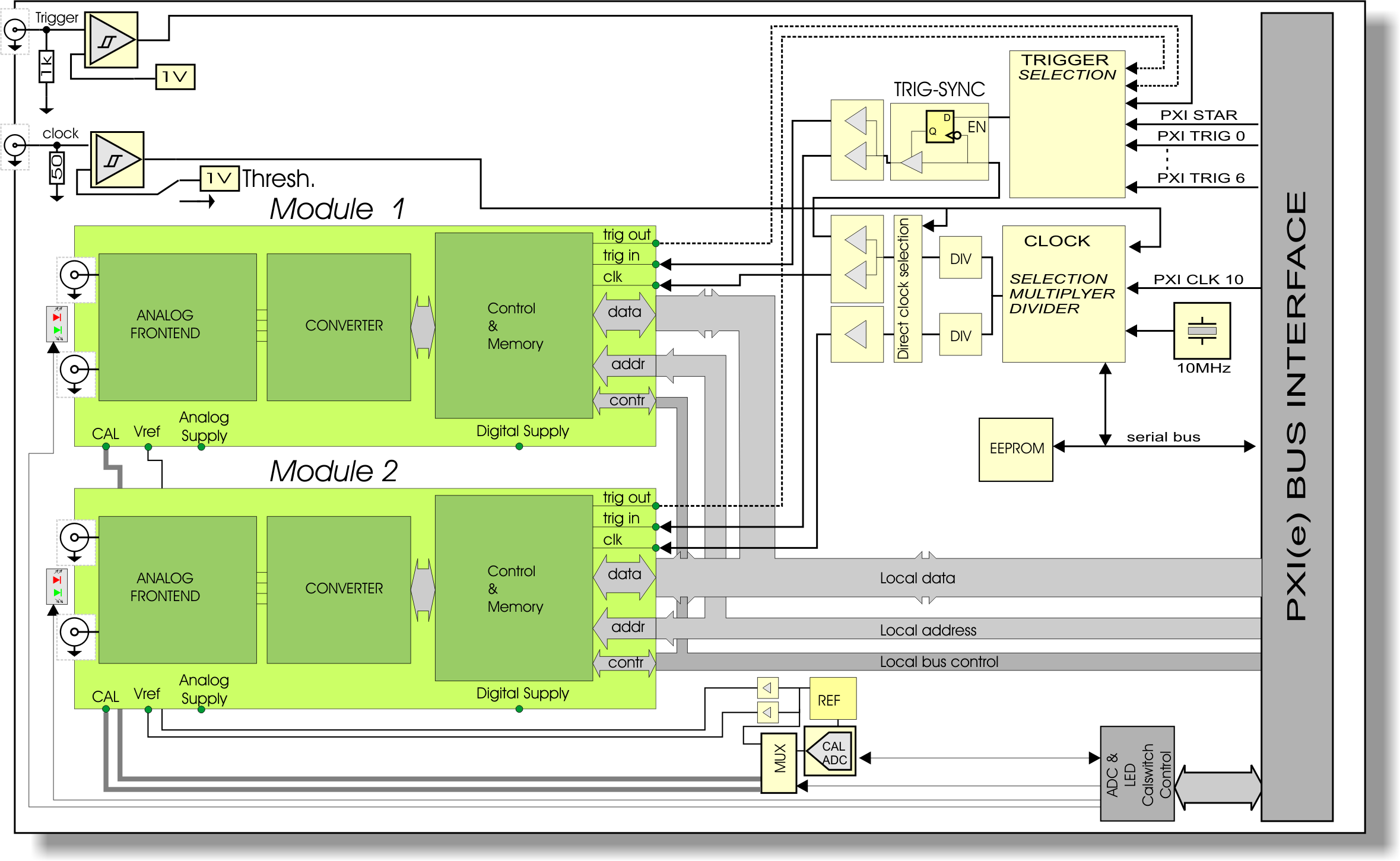
The PA72 base board contains a clock generator, trigger circuitry, a digital voltmeter and the PXI bus interface. In the block diagram below, the base board functions are yellow and the daughter board functions are green. The clock generator is a low jitter PLL clock that has less than 0.5ps jitter for low loop filter bandwidths. With higher loop filter bandwidths, frequency settling time can be less than 250ms.The main clock frequency ranges from 2kHz up to 945MHz with a resolution of less than 1 kHz. Each daughter board slot has its own clock divider.Therefore the clock for each daughter board can be different while maintaining proper synchronization. The PLL clock generator features a high stability, low noise and low jitter 10MHz on-board reference clock with 1ppm frequency stability. In addition the PLL can be locked to the PXI backplane clock or to an external reference clock. The on-board clock source can also be bypassed by an external direct clock.
The trigger input supports edge and level triggering and positive and negative going trigger signals. The trigger source can be software, PXI Star trigger, PXI Trigger 0-6 (3-6 inverted), or external (front). Additionally, digitizer boards can be set to edge-trigger on the analog input signal.
Block Diagram
Key Features
- This is the 1st item
- This is the 2nd item
- Flexible analog signal generation and capture platform
- Two daughter board slots
- Choose daughter boards from the 7 available types
- On-board high accuracy voltmeter
- On-board high performance clock source
- 1ppm clock stability / 0.5ps clock jitter
- Available for PXI and PXI Express
- LabView and LabWindows/CVI (VXIplug&play compatible) drivers included
Available Daughter Boards
Generators
- PA72G16400 - 16 Bit / 400 MS/s Arbitrary Waveform Generator
- PA72G14180 - 14 Bit / 180 MS/s Arbitrary Waveform Generator
Digitizers
- PA72D16180A - 16 Bit / 180 MS/s Digitizer
- PA72D14130 - 14 Bit / 130 MS/s Digitizer
Miscellaneous
- PA72DIOS6016 - Multifunctional programmable Digital I/O
- PA72BPF - Dual Differential Band Pass Filter
Technical Specifications
PLL clock
| Frequency range | 2kHz to 945MHz |
| Sync possibilities | 10MHz backplane or 10MHz external clock |
| PLL lock time | 250ms - 1s (depending on loop filter BW) |
| Jitter | 0.5ps typical |
External clock input
| Clock rate | DC to 500MHz |
| Treshold level | 0V or 1V (programmable) |
| Input impedance | 50 Ohm |
Front trigger input
| Threshold level | 1 V |
| Input impedance | 1k Ohm |
| Max input level | -0.5 V to +5.5 V |
| Coupling | DC |
Trigger sources
Digitizer's analog level trigger, Front trigger input, PXI Star, PXI Trig 0..6, Software triggerBus interface
| PA72 bus | 32-bit PXI, burst mode support |
| PA72e bus | x1 PXI Express, burst mode support |
| Max. burst data rate | 132 MByte/s |